Project for electrical and electronic engineering

Sunday, February 26, 2006

IC Model Making

Introduction

The model IC is an enlarge version of the 74LS86 IC. It is enlarged 8000 times. It has a cut through transparent part located above the model and shows the interial part, magnified 8000x15 times compared to the real wafer chip.

Material selection

The model uses black cardboard as the body of the IC, aluminium sheet as the IC pins, aluminium foil as the internal wiring inside the IC and for the wafer chip components, and green paper for the base of wafer chip.

Building the Model

The model is builded by group member Lucerne. He build both the body and the interial part of the IC. The IC pins are done by me (Loh Yung Jia).


An unfinished IC model showing the interior part.


Presentation

Poster

Below is our poster presentation, which is done by our group member Lim Chun Yap. The photo inside the poster is courtesy of me (Loh Yung Jia).

Friday, February 10, 2006

From Conception to Completion

Testing

After the last component had been soldered in place, the circuit was tested. On the veroboard, a small section of connection in between the pins of IC was cut to avoid short circuit. A 5V power supply was connected to the circuit. A truth table containing 16 combinations of possible 4-bit binary and its constituent Gray code was prepared. The power supply was on and all combinations were tested using the circuit. All components are working fine, the outputs are perfectly correct and match with the truth table. From the initial design of the circuit, to the completion of the circuit, took us only 1 week, and it succeed in the first attempt. 1 week of hard work and dedication has paid off, thanks to the cooperation of group members. All of us are so overjoyed.

Modification

This modification is not an error correction. It is to improve the portability of the design and to improve the physical appearance. A lab assistant of the EE Lab had observed our circuit and suggested that we replace our LEDs wires with a longer, flexible wire so that it can be bent and packed together nicely, rather than using the initial wires that are shorter and inflexible. All wires connecting the LEDs and the switches to the veroboard have to be removed and replaced with the new wires. He also insisted that we replace our LEDs(very dim and cheap) with a brighter one. The new LEDs have 2 colours: green & red(old one shows green only). It is brighter and looks nicer. We set the green LEDs as input indicators, red as output. The modification was all done by me at home, helped by group members at the lab. After 2 hours of modification at home, the circuit is now physically appealing. I had also added the power supply circuit containing capacitors, transistor and battery on the veroboard. Now, the design is completely portable and does not need to rely on fixed power suppply unit.


Top: circuit design before modification
Bottom: circuit design after modification

2nd Testing

The board is tested again to make sure that no error occurs after modification. The circuit work successfully. It is fully portable and is ready for packaging. The specification of the circuit is shown below:
4-bit binary to Gray code converter.
Powered by 74LS86 IC
5V power supply
Support up to 5-bit conversion(upgradable)

Project Progression

Obtaining Materials

After completing the initial design of the circuit, the next thing is to obtain the components needed in the circuit. During the CNY holiday period, group member Lim Chun Yap had bought LEDs, wires, veroboard, IC 74LS86, two-pole switch and solder at Ipoh. On the 7th of February, Lim Chun Yap and Lucerne went to Jalan Pasar to puchase resistors, capacitors, transistor and battery. All materials are prepared and ready to be fitted into the veroboard.

Left: Veroboard, IC and switches
Right: solder, wires and LEDs

Fixing Components

The process of putting all the components onto the veroboard based on the circuit diagram was done by me. After 2 hours of hard work, all the components had been put in place in the veroboard and are ready to be soldered. Electrical and Electronic(EE) Lab was borrowed to do the soldering. Most soldering was done by me with the help of group members. Eventually, the soldered design was completed.

The 74LS86 IC

What is it?

This IC is a quad two-input exclusive OR gates (XOR Gates) IC, which resembles 4 XOR gates inside. This IC works at a voltage of 5V. It has a total of 14 pins, 8 pins for input, 4 pins for output, and 2 pins for voltage. Pin 1, 2, 4, 5, 9, 10, 12, and 13 are inputs, pin 3, 6, 8, and 11 are outputs, pin 7 and 14 are connected to voltage supply. Below is the position of XOR Gates inside the IC:

Arrangement of XOR Gates inside IC 74LS86

About XOR Gate

Exclusive OR Gate, or XOR Gate, is a logic gate that register output HIGH when one of the 2 inputs are DIFFERENT, and register LOW when both inputs are the SAME. Below is the symbol of XOR gate, its Boolean expression & its truth table:

Symbol, Boolean expression & truth table for XOR Gate

This is the circuit for an XOR gate. We can assume that this circuit exist inside the IC. It shows the connection of pin-1, pin-2, pin-3, pin-7 & pin-14. It is said to have 4 similar circuits inside the IC(because it has 4 XOR Gate). Pin-1 and pin-2 are input, pin-3 is output, pin-7 and pin-14 are connected to voltage supply (all 4 XOR gates share the same voltage pins).

Circuit of XOR Gate

Thursday, February 09, 2006

About Gray Code

What is Gray Code?

A Gray code is an encoding of numbers so that adjacent numbers have a single digit differing by 1. The term Gray code is often used to refer to a "reflected" code, or more specifically still, the binary reflected Gray code.
Gray codes were originally designed to prevent spurious output from electromechanical switches. The code was designed by Bell Labs researcher Frank Gray and patented in 1953.

Uses of Gray Code

Gray codes are used in angle-measuring devices in preference to straightforward binary encoding. This avoids the possibility that, when several bits change in the binary representation of an angle, a misread could result from some of the bits changing before others. This application benefits from the cyclic nature of Gray codes, because the first and last values of the sequence differ by only one bit.

The binary-reflected Gray code can also be used to serve as a solution guide for the Tower of Hanoi problem. A detailed method may be found here. It also forms a Hamiltonian cycle on a hypercube, where each bit is seen as one dimension.

Due to the Hamming distance properties of Gray codes, they are sometimes used in Genetic Algorithms. They are very useful in this field, since mutations in the code allow for mostly incremental changes, but occasionally a single bit-change can cause a big leap and lead to new properties.

Gray codes are also used in labelling the axes of Karnaugh maps.

When Gray codes are used in computers to address program memory, the computer uses less power because fewer address lines change as the program counter advances.

Sources: http://mathworld.wolfram.com/GrayCode.html
http://en.wikipedia.org/wiki/Gray_code

Conversion Table

Below is the BCD to Gray Code conversion table, drawn by me.

Review of the Project

Initial Planning

Our group had planned to design a binary code(BCD) to Gray code converter. This idea was first proposed by me(Loh Yung Jia). At first we thought that it was very easy to do it, because we had learned it in one of our lecture. In order to convert 3 bits binary to Gray code, it requires 2 XNOR gates. So, we decided to convert 4 bits, which requires 3 XNOR gates. The IC used in the converter is a quad two-input XNOR gates IC(74LS86). An initial schematic circuit diagram was proposed & drawn by me. The diagram is then checked by Mr. Lee, lecturers of electronic engineering. The initial design faced some problems: it lacks some components. By adding these additional components, the schematic circuit diagram is then drawn and checked by Mr. Lee. Eventually, the design should be working.

Details of the design

This converter containes 8 L.E.D.s, 12 resistors, 3 capacitors, 4 two-pole switches, 1 IC(74LS86), a transistor() and a 9V battery. The 4 switches provide the input of 4 bit binary code. Switch ON=input logic 1, switch OFF=input logic 0. There are 16 possible combination of inputs for a 4-bits binary code. The 4 input LEDs(green) indicates the code that user input. LED ON=logic 1, LED OFF=logic 0. The resulting Gray code is shown by another set of 4 LEDs(red).


Schematic diagram of circuit

Monday, February 06, 2006

Project Planning Chart & Design Proposal

Project Planning Chart (PPC)

Below is the suggested project planning chart which will be updated regularly.
Last update: 4 March 2006

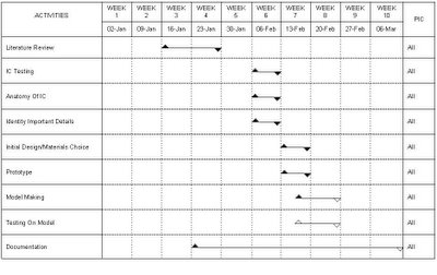
Hollow triangulars represent proposed period.
Solid triangulars represent actual period.


Design proposal

Below is our design proposal: